


Universal DC-DC Convertor
Design : ancEmail: anc
Descriptipn:
This circuit will generate a smaller DC output voltage from a larger DC input voltage.It is quick and simple to make and by changing the value of the zener diode, the circuit can be universally adapted to provide other output voltages.The circuit and all diagrams represent a DC convertor with 12V battery input and 9Volt DC output.
The output voltage is equal to the zener diode voltage less 0.7 volts, or :-
Vo = Vz - 0.7 where V
z is the value of the zener diode.
With the 10V zener diode as shown in the diagram the output voltage is about 9.3 Volts DC. The supply voltage used must always be at least a few volts higher than the zener voltage. In this example I have used a 12 Volt DC battery to provide the regulated 9 Volt DC output.
Output Regulation Versus Input Voltage
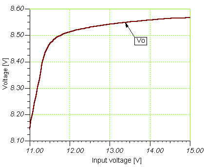
The above graph shows how the output is affected by input voltage variations. This was produced with a load current of 100mA and using a 10 volt rated zener diode. Note that the circuit falls sharply out of regulation when the input voltage falls to 11.5 volt, hence the requirement for an adequate supply voltage.
Temperature Stability
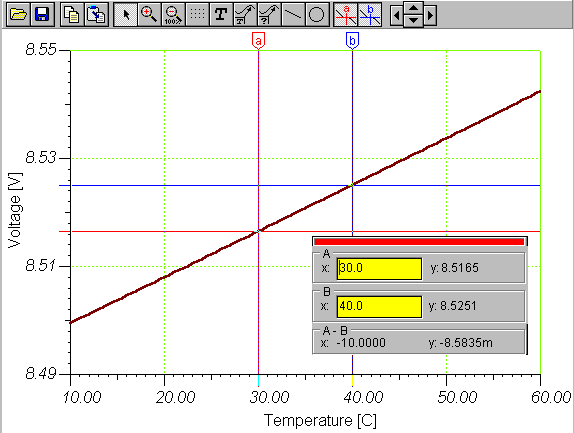
Temperature stability is very good as the above graph shows. The output voltage changes by 8.5mV for every 10 degree rise in temperature. This is less than 1 mV / degree.
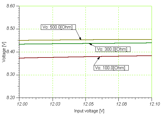
Output Voltage versus Load Current
Power Dissipation
With a DC-DC convertor, the most important consideration is power dissipation in the output device. Power dissipation is the product of the transistors emitter current and collector-emitter voltage. With this circuit the maximum power dissipation of the BD139 or maximum collector current cannot be exceeded, otherwise the transistor will be destroyed.
Example:
With a 12 Volt supply and a 9 Volt, 100 mA load the dissipation is as follows. Using a 10 volt zener the output voltage will be about 9.3 volts DC therefore:
VCE * IC = (12 - 9.3) * 100 mA = 2.7 Watts
This is well within the maximum limits of power dissipation and collector current, which for the BD139 are 8 watts and 1 amp respectively. If higher load currents are required then the following circuit may be used.
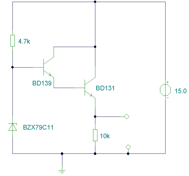
Output dissipation is calculated in the same way, the BD131 has a maximum power dissipation of 15 watts and collector current of 3 amps. The output voltage is approximately 1.4 volts less than the zener diode voltage and supply voltage must be higher than the input voltage by at least 3 volts.
Source:www.zen22142.zen.co.uk