Keys Finder
Source: www.electronics-lab.com
|
Description:
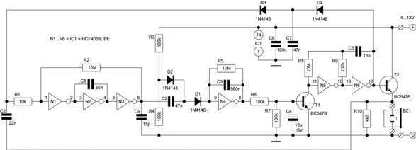
The ear and mouth of the circuit is a piezoelectric buzzer. Fizzling in a frequency of 3...4 KHz produced sound waves that piezoelectric buzzer converts them to an oscillation. This oscillation passes thought C1 and thought inverters N1...N3.The inverters along with R1 and R2, compose an amplifier with gain 400 ! .The C8 and C9 stabilize and reduce the signal's level.
Next the signal rectified from D2 and D3. The integral circuit Н4, C3 and R5 ensures that the circuit will not triggered from common noises but only from late fizzle. When the output voltage increases at N4, Ф1 cuts off and the input of Н4 goes to high logical level. It's output goes to <0> and C5 is charged, through R9 until N5 changes operation state.
Click on the image for the full version.
Next C5 discharges and everything is starting from beginning .The AC voltage goes thought the buffer circuit of T2 to buzzer witch starts to fizzle. There is a small problem in this point, the buzzer will never stop fizzling because the output signal triggering the circuit again thought C1. This is solved in this way: when the buzzer sounds (until C3 discharges thought R5), the input of Н1 goes through D4, C7 and D3, to high logical state. In this way until the buzzer stops the input of the amplifier can't receive and amplify any given signal.
Parts
R1 =10k R2, R5, R8 =10M R3, R4, R6, R7, R9 = 100k R10 = 4k7 C1 = 22n C2, C7 = 47n C3 = 560n C4 = 10м/16V Tantalum C5 = 1n5 C6 = 100n C8 = 56n C9 = 15p D1...D4 = 1N4148 T1, T2 = BC547B IC1 = HCF4069UBE
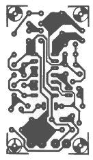
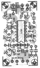
PCB


