


ISA bus
pinout
ISA=Industry Standard Architecture
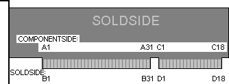
 98 pin (62+36)ISA EDGE male connector at the card |
The AT version of the bus is upwardly compatible, which means that cards designed to work on an XT bus will work on an AT bus. This bus was produced for many years without any formal standard. In recent years, a more formal standard called the ISA bus (Industry Standard Architecture) has been created, with an extension called the EISA (Extended ISA) bus also now as a standard. The EISA bus extensions will not be detailed here. This file is not intended to be a thorough coverage of the standard. It is for informational purposes only, and is intended to give designers and hobbyists sufficient information to design their own XT and AT compatible cards. Physical Design:ISA cards can be either 8-bit or 16-bit. 8-bit cards only uses the first 62 pins and 16-bit cards uses all 98 pins. Some 8-bit cards uses some of the 16-bit extension pins to get more interrupts. 16-bit card:
Signal Descriptions:+5, -5, +12, -12Power supplies. -5 is often not implemented. AENAddress Enable. This is asserted when a DMAC has control of the bus. This prevents an I/O device from responding to the I/O command lines during a DMA transfer. When AEN is active, the DMA Controller has control of the address bus as the memory and I/O read/write command lines. BALEBus Address Latch Enable. The address bus is latched on the rising edge of this signal. The address on the SA bus is valid from the falling edge of BALE to the end of the bus cycle. Memory devices should latch the LA bus on the falling edge of BALE. Some references refer to this signal as Buffered Address Latch Enable, or just Address Latch Enable (ALE). The Buffered-Address Latch Enable is used to latch SA0-19 on the falling edge. This signal is forced high during DMA cycles. BCLKBus Clock, 33% Duty Cycle. Frequency Varies. 4.77 to 8 MHz typical. 8.3 MHz is specified as the maximum, but many systems allow this clock to be set to 12 MHz and higher. DACKxDMA Acknowledge. The active-low DMA Acknowledge 0 to 3 and 5 to 7 are the corresponding acknowledge signals for DRQ 0-3, 5-7. DRQxDMA Request. These signals are asynchronous channel requests used by I/O channel devices to gain DMA service. DMA request channels 0-3 are for 8-bit data transfer. DAM request channels 5-7 are for 16-bit data transfer. DMA request channel 4 is used internally on the system board. DMA requests should be held high until the corresponding DACK line goes active. DMA requests are serviced in the following priority sequence: IOCS16I/O size 16. Generated by a 16 bit slave when addressed by a bus master. The active-low I/O Chip Select 16 indicates that the current transfer is a 1 wait state, 16 bit I/O cycle. Open Collector. I/O CH CKChannel Check. A low signal generates an NMI. The NMI signal can be masked on a PC, externally to the processor (of course). Bit 7 of port 70(hex) (enable NMI interrupts) and bit 3 of port 61 (hex) (recognition of channel check) must both be set to zero for an NMI to reach the cpu. The I/O Channel Check is an active-low signal which indicates that a parity error exists in a device on the I/O channel. I/O CH RDYChannel Ready. Setting this low prevents the default ready timer from timing out. The slave device may then set it high again when it is ready to end the bus cycle. Holding this line low for too long (15 microseconds, typical) can prevent RAM refresh cycles on some systems. This signal is called IOCHRDY (I/O Channel Ready) by some references. CHRDY and NOWS should not be used simultaneously. This may cause problems with some bus controllers. This signal is pulled low by a memory or I/O device to lengthen memory or I/O read/write cycles. It should only be held low for a minimum of 2.5 microseconds. IORThe I/O Read is an active-low signal which instructs the I/O device to drive its data onto the data bus, SD0-SD15. IOWThe I/O Write is an active-low signal which instructs the I/O device to read data from the data bus, SD0-SD15. IRQxInterrupt Request. IRQ2 has the highest priority. IRQ 10-15 are only available on AT machines, and are higher priority than IRQ 3-7. The Interrupt Request signals which indicate I/O service attention. They are prioritized in the following sequence: Highest IRQ 9(2),10,11,12,14,3,4,5,6,7 LAxxLatchable Address lines. Combine with the lower address lines to form a 24 bit address space (16 MB) These unlatched address signals give the system up to 16 MB of address ability. The are valid when "BALE" is high. MASTER16 bit bus master. Generated by the ISA bus master when initiating a bus cycle. This active-low signal is used in conjunction with a DRQ line by a processor on the I/O channel to gain control of the system. The I/O processor first issues a DRQ, and upon receiving the corresponding DACK, the I/O processor may assert MASTER, which will allow it to control the system address, data and control lines. This signal should not be asserted for more than 15 microseconds, or system memory may be corrupted du to the lack of memory refresh activity. MEMCS16The active-low Memory Chip Select 16 indicates that the current data transfer is a 1 wait state, 16 bit data memory cycle. MEMRThe Memory Read is an active-low signal which instructs memory devices to drive data onto the data bus SD0-SD15. This signal is active on all memory read cycles. MEMWThe Memory Write is an active-low signal which instructs memory devices to store data present on the data bus SD0-SD15. This signal is active on all memory write cycles. NOWSNo Wait State. Used to shorten the number of wait states generated by the default ready timer. This causes the bus cycle to end more quickly, since wait states will not be inserted. Most systems will ignore NOWS if CHRDY is active (low). However, this may cause problems with some bus controllers, and both signals should not be active simultaneously. OSCOscillator, 14.31818 MHz, 50% Duty Cycle. Frequency varies. This was originally divided by 3 to provide the 4.77 MHz cpu clock of early PCs, and divided by 12 to produce the 1.19 MHz system clock. Some references have placed this signal as low as 1 MHz (possibly referencing the system clock), but most modern systems use 14.318 MHz. REFRESHRefresh. Generated when the refresh logic is bus master. This active-low signal is used to indicate a memory refresh cycle is in progress. An ISA device acting as bus master may also use this signal to initiate a refresh cycle. RESETThis signal goes low when the machine is powered up. Driving it low will force a system reset. This signal goes high to reset the system during powerup, low line-voltage or hardware reset. ?????????????? SA0-SA19System Address Lines, tri-state. The System Address lines run from bit 0 to bit 19. They are latched on to the falling edge of "BALE". SBHESystem Bus High Enable, tristate. Indicates a 16 bit data transfer. The System Bus High Enable indicates high byte transfer is occurring on the data bus SD8-SD15. This may also indicate an 8 bit transfer using the upper half of the bus data (if an odd address is present). SD0-SD16System Data lines, or Standard Data Lines. They are bidrectional and tri-state. On most systems, the data lines float high when not driven. These 16 lines provide for data transfer between the processor, memory and I/O devices. SMEMRSystem Memory Read Command line. Indicates a memory read in the lower 1 MB area. This System Memory Read is an active-low signal which instructs memory devices to drive data onto the data bus SD0-SD15. This signal is active only when the memory address is within the lowest 1MB of memory address space. SMEMWSystem Memory Write Commmand line. Indicates a memory write in the lower 1 MB area. The System Memory Write is an active-low signal which instructs memory devices to store data preset on the data bus SD0-SD15. This signal is active only when the memory address is within the lowest 1MB of memory address space. T/CTerminal Count. Notifies the cpu that that the last DMA data transfer operation is complete. Terminal Count provides a pulse when the terminal count for any DMA channel is reached. 8 Bit Memory or I/O Transfer Timing Diagram (4 wait states shown) __ __ __ __ __ __ __
BCLK ___| |___| |___| |__| |___| |___| |___| |__
W1 W2 W3 W4
__
BALE _______| |_______________________________________
AEN __________________________________________________
______________________________________
SA0-SA19 ---------<______________________________________>-
_____________ _____
Command Line |______________________________|
(IORC,IOWC,
SMRDC, or SMWTC)
_____
SD0-SD7 ---------------------------------------<_____>----
(READ)
___________________________________
SD0-SD7 ---------<___________________________________>----
(WRITE)Note: W1 through W4 indicate wait cycles. BALE is placed high, and the address is latched on the SA bus. The slave device may safely sample the address during the falling edge of BALE, and the address on the SA bus remains valid until the end of the transfer cycle. Note that AEN remains low throughout the entire transfer cycle. The command line is then pulled low (IORC or IOWC for I/O commands, SMRDSC or SMWTC for memory commands, read and write respectively). For write operations, the data remains on the SD bus for the remainder of the transfer cycle. For read operations, the data must be valid on the falling edge of the last cycle. NOWS is sampled at the midpoint of each wait cycle. If it is low, the transfer cycle terminates without further wait states. CHRDY is sampled during the first half of the clock cycle. If it is low, further wait cycles will be inserted. The default for 8 bit transfers is 4 wait states. Some computers allow the number of default wait states to be changed. 16 Bit Memory or I/O Transfer Timing Diagram (1 wait state shown)
                  __     __     __    __     __     __
BCLK          ___|  |___|  |___|  |__|  |___|  |___|  |_


AEN [2]       __________________________________________

                      _____________
LA17-LA23     -------<_____________>-[1]-----------------

                             __
BALE          ______________|  |________________________

             ________________                    _______
SBHE                         |__________________|

                              __________________
SA0-SA19      ---------------<__________________>-------

             _________________      ____________________
M16                           |____|
                               *  * [4]

             _________________               ___________
IO16 [3]                      |_____________|
                                        *

              _________________              ___________
Command Line                   |____________|
(IORC,IOWC,
MRDC, or MWTC)
                                          ____
SD0-SD7       ---------------------------<____>---------
(READ)

                                ______________
SD0-SD7       -----------------<______________>---------
(WRITE)
An asterisk (*) denotes the point where the signal is sampled. [1] The portion of the address on the LA bus for the NEXT cycle may now be placed on the bus. This is used so that cards may begin decoding the address early. Address pipelining must be active. [2] AEN remains low throughout the entire transfer cycle, indicating that a normal (non-DMA) transfer is occurring. [3] Some bus controllers sample this signal during the same clock cycle as M16, instead of during the first wait state, as shown above. In this case, IO16 needs to be pulled low as soon as the address is decoded, which is before the I/O command lines are active. [4] M16 is sampled a second time, in case the adapter card did not active the signal in time for the first sample (usually because the memory device is not monitoring the LA bus for early address information, or is waiting for the falling edge of BALE). 16 bit transfers follow the same basic timing as 8 bit transfers. A valid address may appear on the LA bus prior to the beginning of the transfer cycle. Unlike the SA bus, the LA bus is not latched, and is not valid for the entire transfer cycle (on most computers). The LA bus should be latched on the falling edge of BALE. Note that on some systems, the LA bus signals will follow the same timing as the SA bus. On either type of system, a valid address is present on the falling edge of BALE. I/O adapter cards do not need to monitor the LA bus or BALE, since I/O addresses are always within the address space of the SA bus. SBHE will be pulled low by the system board, and the adapter card must respond with IO16 or M16 at the appropriate time, or else the transfer will be split into two separate 8 bit transfers. Many systems expect IO16 or M16 before the command lines are valid. This requires that IO16 or M16 be pulled low as soon as the address is decoded (before it is known whether the cycle is I/O or Memory). If the system is starting a memory cycle, it will ignore IO16 (and vice-versa for I/O cycles and M16). For read operations, the data is sampled on the rising edge of the last clock cycle. For write operations, valid data appears on the bus before the end of the cycle, as shown in the timing diagram. While the timing diagram indicates that the data needs to be sampled on the rising clock, on most systems it remains valid for the entire clock cycle. The default for 16 bit transfers is 1 wait state. This may be shortened or lengthened in the same manner as 8 bit transfers, via NOWS and CHRDY. Many systems only allow 16 bit memory devices (and not I/O devices) to transfer using 0 wait states (NOWS has no effect on 16 bit I/O cycles). SMRDC/SMWTC follow the same timing as MRDC/MWTC respectively when the address is within the lower 1 MB. If the address is not within the lower 1 MB boundary, SMRDC/SMWTC will remain high during the entire cycle. It is also possible for an 8 bit bus cycle to use the upper portion of the bus. In this case, the timing will be similar to a 16 bit cycle, but an odd address will be present on the bus. This means that the bus is transferring 8 bits using the upper data bits (SD8-SD15). Shortening or Lengthening the bus cycle:BCLK W W W W
_ __ __ __ __ __ __ __ __ __ __ __
|__| |__| |__| |__| |__| |__| |__| |__| |__| |__| |__| |__
|--Transfer 1-----|----Transfer 2---------|----Transfer 3---|
BALE
__ __ __ __
________| |______________| |____________________| |______________|
SBHE
_________ _______________________
|__________________|__________________|
SA0-SA19
_________________ _____________________ _________________
----------<_________________><_____________________><_________________>
IO16
___________ ___ ___________________________
|_____________| |_____________|
* *
CHRDY
________________________________ _______________________________
|______|
* * * [1]
NOWS
______________________________________________________ _____
|__________|
* [2]
IORC
______________ _______ _______ ____
|_________| |_______________| |_________|
SD0-SD15
____ ____ ____
--------------------<____>------------------<____>------------<____>---
* * *An asterisk (*) denotes the point where the signal is sampled. This timing diagram shows three different transfer cycles. The first is a 16 bit standard I/O read. This is followed by an almost identical 16 bit I/O read, with one wait state inserted. The I/O device pulls CHRDY low to indicate that it is not ready to complete the transfer (see [1]). This inserts a wait cycle, and CHRDY is again sampled. At this second sample, the I/O device has completed its operation and released CHRDY, and the bus cycle now terminates. The third cycle is an 8 bit transfer, which is shortened to 1 wait state (the default is 4) by the use of NOWS. I/O Port AddressesNote: Only the first 10 address lines are decoded for I/O operations. This limits the I/O address space to address 3FF (hex) and lower. Some systems allow for 16 bit I/O address space, but may be limited due to some I/O cards only decoding 10 of these 16 bits.
Soundblaster cards usually use I/O ports 220-22F. DMA Read and WriteThe ISA bus uses two DMA controllers (DMAC) cascaded together. The slave DMAC connects to the master DMAC via DMA channel 4 (channel 0 on the master DMAC). The slave therefore gains control of the bus through the master DMAC. On the ISA bus, the DMAC is programmed to use fixed priority (channel 0 always has the highest priority), which means that channel 0-4 from the slave have the highest priority (since they connect to the master channel 0), followed by channels 5-7 (which are channel 1-3 on the master). The DMAC can be programmed for read transfers (data is read from memory and written to the I/O device), write transfers (data is read from the I/O device and written to memory), or verify transfers (neither a read or a write - this was used by DMA CH0 for DRAM refresh on early PCs). Before a DMA transfer can take place, the DMA Controller (DMAC) must be programmed. This is done by writing the start address and the number of bytes to transfer (called the transfer count) and the direction of the transfer to the DMAC. After the DMAC has been programmed, the device may activate the appropriate DMA request (DRQx) line. Slave DMA Controller
Master DMA Controller
Single Transfer ModeThe DMAC is programmed for transfer. The DMA device requests a transfer by driving the appropriate DRQ line high. The DMAC responds by asserting AEN and acknowledges the DMA request through the appropriate DAK line. The I/O and memory command lines are also asserted. When the DMA device sees the DAK signal, it drops the DRQ line. The DMAC places the memory address on the SA bus (at the same time as the command lines are asserted), and the device either reads from or writes to memory, depending on the type of transfer. The transfer count is incremented, and the address incremented/decremented. DAK is de-asserted. The cpu now once again has control of the bus, and continues execution until the I/O device is once again ready for transfer. The DMA device repeats the procedure, driving DRQ high and waiting for DAK, then transferring data. This continues for a number of cycles equal to the transfer count. When this has been completed, the DMAC signals the cpu that the DMA transfer is complete via the TC (terminal count) signal.
                  __     __     __    __     __     __
BCLK          ___|  |___|  |___|  |__|  |___|  |___|  |___

               _______
DRQx         _|       |___________________________________

                   ______________________________
AEN           ____|                              |________

              _______                             ________
DAKx                 |___________________________|

                      ____________________________
SA0-SA15      -------<____________________________>-------


              ___________                     ____________
Command Line             |___________________|
(IORC, MRDC)
                                     _____________
SD0-SD7       ----------------------<_____________>-------
(READ)

                      ____________________________
SD0-SD7       -------<____________________________>-------
(WRITE)
Block Transfer ModeThe DMAC is programmed for transfer. The device attempting DMA transfer drives the appropriate DRQ line high. The motherboard responds by driving AEN high and DAK low. This indicates that the DMA device is now the bus master. In response to the DAK signal, the DMA device drops DRQ. The DMAC places the address for DMA transfer on the address bus. Both the memory and I/O command lines are asserted (since DMA involves both an I/O and a memory device). AEN prevents I/O devices from responding to the I/O command lines, which would not result in proper operation since the I/O lines are active, but a memory address is on the address bus. The data transfer is now done (memory read or write), and the DMAC increments/decrements the address and begins another cycle. This continues for a number of cycles equal to the DMAC transfer count. When this has been completed, the terminal count signal (TC) is generated by the DMAC to inform the cpu that the DMA transfer has been completed. Note: Block transfer must be used carefully. The bus cannot be used for other things (like RAM refresh) while block mode transfers are being done. Demand Transfer ModeThe DMAC is programmed for transfer. The device attempting DMA transfer drives the appropriate DRQ line high. The motherboard responds by driving AEN high and DAK low. This indicates that the DMA device is now the bus master. Unlike single transfer and block transfer, the DMA device does not drop DRQ in response to DAK. The DMA device transfers data in the same manner as for block transfers. The DMAC will continue to generate DMA cycles as long as the I/O device asserts DRQ. When the I/O device is unable to continue the transfer (if it no longer had data ready to transfer, for example), it drops DRQ and the cpu once again has control of the bus. Control is returned to the DMAC by once again asserting DRQ. This continues until the terminal count has been reached, and the TC signal informs the cpu that the transfer has been completed. Interrupts on the ISA bus
IRQ0,1,2,8, and 13 are not available on the ISA bus. The IBM PC and XT had only a single 8259 interrupt controller. The AT and later machines have a second interrupt controller, and the two are used in a master/slave combination. IRQ2 and IRQ9 are the same pin on most ISA systems. Interrupts on most systems may be either edge triggered or level triggered. The default is usually edge triggered, and active high (low to high transition). The interrupt level must be held high until the first interrupt acknowledge cycle (two interrupt acknowledge bus cycles are generated in response to an interrupt request). The software aspects of interrupts and interrupt handlers is intentionally omitted from this document, due to the numerous syntactical differences in software tools and the fact that adequate documentation of this topic is usually provided with developement software. Bus Mastering:An ISA device may take control of the bus, but this must be done with caution. There are no safety mechanisms involved, and so it is easily possible to crash the entire system by incorrectly taking control of the bus. For example, most systems require bus cycles for DRAM refresh. If the ISA bus master does not relinquish control of the bus or generate its own DRAM refresh cycles every 15 microseconds, the system RAM can become corrupted. The ISA adapter card can generate refresh cycles without relinquishing control of the bus by asserting REFRESH. MRDC can be then monitored to determine when the refresh cycle ends. To take control of the bus, the device first asserts its DRQ line. The DMAC sends a hold request to the cpu, and when the DMAC receives a hold acknowledge, it asserts the appropriate DAK line corresponding to the DRQ line asserted. The device is now the bus master. AEN is asserted, so if the device wishes to access I/O devices, it must assert MASTER16 to release AEN. Control of the bus is returned to the system board by releasing DRQ. Sources: Mark Sokos ISA pageSources: "ISA System Architecture, 3rd Edition" by Tom Shanley and Don Anderson ISBN 0-201-40996-8 Sources: "Eisa System Architecture, 2nd Edition" by Tom Shanley and Don Anderson ISBN 0-201-40995-X Sources: "Microcomputer Busses" by R.M. Cram ISBN 0-12-196155-9 Sources: HelpPC v2.10 Quick Reference Utility, by David Jurgens Sources: ZIDA 80486 Mother Board User"s Manual, OPTi 486, 82C495sx Note: Direction is Motherboard relative ISA-Cards. Source:www.pinouts.ru |
 (At the card)
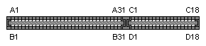 (At the computer)