


EISA bus
pinout
This file is intended to provide a basic functional overview of the EISA Bus, so that hobbyists and amateurs can design their own EISA compatible cards.
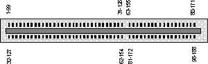 198 pin (62+36/62+38) EISA EDGE connector at the computer (as a sample, wrong numbering) | EISA=Extended Industry Standard Architecture. This file is intended to provide a basic functional overview of the EISA Bus, so that hobbyists and amateurs can design their own EISA compatible cards. It is not intended to provide complete coverage of the EISA standard. EISA is an acronym for Extended Industry Standard Architecture. It is an extension of the ISA architecture, which is a standardized version of the bus originally developed by IBM for their PC computers. EISA is upwardly compatible, which means that cards originally designed for the 8 bit IBM bus (often referred to as the XT bus) and cards designed for the 16 bit bus (referred to as the AT bus, and also as the ISA bus), will work in an EISA slot. EISA specific cards will not work in an AT or an XT slot. The EISA connector uses multiple rows of connectors. The upper row is the same as a regular ISA slot, and the lower row contains the EISA extension. The slot is keyed so that ISA cards cannot be inserted to the point where they connect with the EISA signals.
+---------------------------------------------+
|            (component side)                 |
|                                             |
|___________ ISA-16bit __       ISA-8bit    __|
            |||||||||||  |||||||||||||||||||  A1(front)/B1(back)
             | | | | |    | | | | | | | | |  EISA: E1(front)/F1(back)
                   C1/D1
                  G1/H1
A,C,E,G=Component Side A,B,F,H=Sold Side
EISA is an acronym for Extended Industry Standard Architecture. It is an extension of the ISA architecture, which is a standardized version of the bus originally developed by IBM for their PC computers. EISA is upwardly compatible, which means that cards originally designed for the 8 bit IBM bus (often referred to as the XT bus) and cards designed for the 16 bit bus (referred to as the AT bus, and also as the ISA bus), will work in an EISA slot. EISA specific cards will not work in an AT or an XT slot. The EISA connector uses multiple rows of connectors. The upper row is the same as a regular ISA slot, and the lower row contains the EISA extension. The slot is keyed so that ISA cards cannot be inserted to the point where they connect with the EISA signals. Signal Descriptions+5, -5, +12, -12Power supplies. -5 is often not implemented. AENAddress Enable. This is asserted when a DMAC has control of the bus. This prevents an I/O device from responding to the I/O command lines during a DMA transfer. BALEBus Address Latch Enable. The address bus is latched on the rising edge of this signal. The address on the SA bus is valid from the falling edge of BALE to the end of the bus cycle. Memory devices should latch the LA bus on the falling edge of BALE. BCLKBus Clock, 33% Duty Cycle. Frequency Varies. 8.33 MHz is specified as the maximum, but many systems allow this clock to be set to 10 MHz and higher. BE(x)Byte Enable. Indicates to the slave device which bytes on the data bus contain valid data. A 16 bit transfer would assert BE0 and BE1, for example, but not BE2 or BE3. CHCHKChannel Check. A low signal generates an NMI. The NMI signal can be masked on a PC, externally to the processor (of course). Bit 7 of port 70(hex) (enable NMI interrupts) and bit 3 of port 61 (hex) (recognition of channel check) must both be set to zero for an NMI to reach the cpu. CHRDYChannel Ready. Setting this low prevents the default ready timer from timing out. The slave device may then set it high again when it is ready to end the bus cycle. Holding this line low for too long can cause problems on some systems. CHRDY and NOWS should not be used simultaneously. This may cause problems with some bus controllers. CMDCommand Phase. This signal indicates that the current bus cycle is in the command phase. After the start phase (see START), the data is transferred during the CMD phase. CMD remains asserted from the falling edge of START until the end of the bus cycle. SD0-SD16System Data lines. They are bidrectional and tri-state. DAKxDMA Acknowledge. DRQxDMA Request. EX16EISA Slave Size 16. This is used by the slave device to inform the bus master that it is capable of 16 bit transfers. EX32EISA Slave Size 32. This is used by the slave device to inform the bus master that it is capable of 32 bit transfers. EXRDYEISA Ready. If this signal is asserted, the cycle will end on the next rising edge of BCLK. The slave device drives this signal low to insert wait states. IO16I/O size 16. Generated by a 16 bit slave when addressed by a bus master. IORCI/O Read Command line. IOWCI/O Write Command line. IRQxInterrupt Request. IRQ2 has the highest priority. LAxxLatchable Address lines. LOCKAsserting this signal prevents other bus masters from requesting control of the bus. MAKxMaster Acknowledge for slot x: Indicates that the bus master request (MREQx) has been granted. MASTER1616 bit bus master. Generated by the ISA bus master when initiating a bus cycle. M/IOMemory/Input-Output. This is used to indicate whether the current bus cycle is a memory or an I/O operation. M16Memory Access, 16 bit MRDCMemory Read Command line. MREQxMaster Request for Slot x: This is a slot specific request for the device to become the bus master. MSBURSTMaster Burst. The bus master asserts this signal in response to SLBURST. This tells the slave device that the bus master is also capable of burst cycles. MWTCMemory Write Command line. NOWSNo Wait State. Used to shorten the number of wait states generated by the default ready timer. This causes the bus cycle to end more quickly, since wait states will not be inserted. Most systems will ignore NOWS if CHRDY is active (low). However, this may cause problems with some bus controllers, and both signals should not be active simultaneously. OSCOscillator, 14.318 MHz, 50% Duty Cycle. Frequency varies. REFRESHRefresh. Generated when the refresh logic is bus master. RESDRVThis signal goes low when the machine is powered up. Driving it low will force a system reset. SA0-SA19System Address Lines, tri-state. SBHESystem Bus High Enable, tristate. Indicates a 16 bit data transfer. SLBURSTSlave Burst. The slave device uses this to indicate that it is capable of burst cycles. The bus master will respond with MSBURST if it is also capable of burst cycles. SMRDCStandard Memory Read Command line. Indicates a memory read in the lower 1 MB area. SMWTCStandard Memory Write Commmand line. Indicates a memory write in the lower 1 MB area. STARTStart Phase. This signal is low when the current bus cycle is in the start phase. Address and M/IO signals are decoded during this phase. Data is transferred during the command phase (indicated by CMD). TCTerminal Count. Notifies the cpu that that the last DMA data transfer operation is complete. W/RWrite or Read. Used to indicate if the current bus cycle is a read or a write operation. Source:www.pinouts.ru |