


VESA LocalBus (VLB)
pinout
VLB=VESA Local Bus. VESA=Video Electronics Standards Association.
 58 pin EDGE male connector at the card | The VESA Local Bus is a local bus defined by the Video Electronics Standards Association, mostly used in personal computers based on the Intel 80486 CPU. VESA Local Bus worked alongside the ISA bus; it acted as a high-speed conduit for memory-mapped I/O and DMA, while the ISA bus handled interrupts and port-mapped I/O. The VESA Local Bus was designed as a stop-gap solution to the problem of the ISA bus"s limited bandwidth. VESA had several flaws that served to limit its useful life substantially: 80486 dependence. The VESA Local Bus relied heavily on the 80486"s memory bus design. When the Pentium processor started to gain mass acceptance, circa 1995, there were major differences in its bus design, and the VESA bus was not easily adaptable. This also made moving the bus to non-Intel architectures nearly impossible. Few Pentium motherboards with VESA slots were ever made. Limited number of slots available. Most PCs that used VESA Local Bus had only one or two slots available, as opposed to 5 or 6 ISA slots. This was because, as a direct branch of the 80486 memory bus, the VESA Local Bus didn"t have the electrical ability to drive more than 1 or 2 (or 3 at the most) cards at a time. Despite these problems, the VESA Local Bus was very commonplace on 486 motherboards. Probably a majority of 486-based systems had a VESA Local Bus video card, although early 486 systems never had VESA slots, as VESA debuted years after the introduction of the 486 processor.
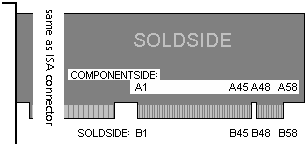
This section is currently based solely on the work by Mark Sokos. This file is intended to provide a basic functional overview of the Vesa Local Bus, so that hobbyists and amateurs can design their own VLB compatible cards. It is not intended to provide complete coverage of the VLB standard. VLB Connectors are usually inline with ISA connectors, so that adapter cards may use both. However, the VLB is separate, and does not need to connect to the ISA portion of the bus. The 64 bit expansion of the bus (optional) does not add additional pins or connectors. Instead, it multiplexes the existing pins. The 32 bit VLB bus does not use the 64 bit signals shown in the above pinouts. Signal DescriptionsA2-A31Address Bus ADSAddress Strobe BE0-BE3Byte Enable. Indicates that the 8 data lines corresponding to each signal will deliver valid data. BLASTBurst Last. Indicates a VLB Burst Cycle, which will complete with *BRDY. The VLB Burst cycle consists of an address phase followed by four data phases. BRDYBurst Ready. Indicates the end of the current burst transfer. D0-D31Data Bus. Valid bytes are indicated by *BE(x) signals. D/CData/Command. Used with M/IO and W/R to indicate the type of cycle.
ID0-ID4Identification Signals.
IRQ9Interrupt Request. Connected to IRQ9 on ISA bus. This allows standalone VLB adapters (not connected to ISA portion of the bus) to have one IRQ. LEADSLocal Enable Address Strobe. Set low by VLB master (not CPU). Also used for cache invalidation signal. LBS16Local Bus Size 16. Used by slave device to indicate that it has a transfer width of only 16 bits. LCLKLocal Clock. Runs at the same frequency as the cpu, up to 50 MHz. 66 MHz is allowed for on-board devices. LDEVLocal Device: When appropriate address and M/IO signals are present on the bus, the VLB device must pull this line low to indicate that it is a VLB device. The VLB controller will then use the VLB bus for the transfer. LRDYLocal Ready. Indicates that the VLB device has completed the cycle. This signal is only used for single cycle transfers. *BRDY is used for burst transfers. LGNTLocal Grant. Indicates that an *LREQ signal has been granted, and control is being transferred to the new VLB master. LREQLocal Request. Used by VLB Master to gain control of the bus. M/IOMemory/IO. See D/C for signal description. RDYRTNReady Return. Indicates VLB cycle has been completed. May precede LRDY by one cycle. RESETReset. Resets all VLB devices. WBACKWrite Back. 64-bit Expansion SignalsACK64Acknowledge 64 bit transfer. Indicates that the device can perform the requested 64 bit transfer cycle. BE4-BE7Byte Enable. Indicates which bytes are valid (similar to BE0-BE3). D32-D63Upper 32 bits of data bus. Multiplexed with address bus. LBS64Local Bus Size 64 bits. Used by VLB Master to indicate that it desires a 64 bit transfer. W/RWrite/Read. See D/C for signal description. 64 Bit Data Transfer Timing Diagram: Address Data
Phase Phase
_______ _______ _______
LCLK ___| |_______| |_______| |_______
____ ______________________________________
*ADS |_______|
_______________ _______________
A2-A31 ----<_______________><_______________>-------------
D34-D63 Address Data D34-D63
_______________ _______________
D/C ----<_______________><_______________>-------------
M/IO, W/R M/IO, W/R Data D32-33
_____ _____________________________
*LDEV |_______________|
_____ _____________________________
*LBS64 |_______________|
______ _____________________________
*ACK64 |______________|
_______________
D0-D31 --------------------<_______________>-------------
_____________________ _____________
LRDY |______________|
|
Source:www.pinouts.ru