Switch-mode Power Supply for a Tube Car Amplifier
(c) klausmobile 2001
Design goals
- +11.0 ... +15.0 V input power supply, undervoltage protection under +11V
- Low-dropout linear heater supply regulated to +11.5 .. +12.0 V (series-wired 6V filaments), 3A (scalable up or down)
- Regulated DCDC plate supply +250..+270V, 300mA, fully isolated from chassis or power input, DC impedance less than 10 Ohm
- Plate supply powerup delay - 20..30s upon REM IN signal (turn-off immediately as REM IN is turned off)
- Muting relay ebable delay 3..5s upon plate supply powerup (turn-off immediately as REM IN is turned off
- Maximum 3W power dissipation on any transistor to simplify heatsinking. In my design, instead of a dedicated heatsink, the PCB is simply bolted tightly against chassis bottom which is the only available sink.
Heater supply and timers
To minimize heat loss on any transistor, I use two pass FETs. In the car, input voltage is either 11.5-12.5V (engine off) or 13.5-14.5V (engine on). In the first case, T1 and T2 are fully ON, no need for heatsink. In the second case - T1 is OFF, T2 ON, all voltage and power excess is released across R5, no heatsink necessary for FETs. However, when input is in between (13...14V) - T1, in a linear regulator mode, may dissipate up to 3W (for a 3A load current).
Parts choice/substitutes:
- Optocouples may be any FET or bipolar output, rated to 5mA output (except for the upper half of IC5) . Upper IC5 optocouple sources power supply to PWM controller IC, which is around 20mA.
- Т1-Т3 сan be any low-voltage FET, Rds<0.1Ohm. I used IRFI540, IRFI9630 - whatever was in a box. Note that I always prefer fully insulated TO220 devices (IRFIxxx code) - this simplifies placement a lot.
- T2-T3 may be of logic-level or 'normal' type FET. T1 must be 'normal' type FET only.
- T3 can be a bipolar PNP type (adjust R12,R13 for proper base current).
- C2 can be anything from 470uF up - it's main purpose is to prevent oscillations.
Plate regulator
I use UC3825 controller chip because it needs no external gate driver, minimizing parts count. Current-mode control is not necessary: in 12V networks, the transistors have at least 5x current margin, so in case of a bad short they will survive before the fuse blows. UC3825 is clocked at 180kHz (transformer-dependent). Filter is a ladder CRCRC (no L's!), voltage feedback is drawn from the second C in this chain. Such arrangement, together with a low error amplifier gain, guarantees stability.R120-T1-D107 current varies within 0-4mA range, so this network itself is an additional shunt regulator (with very narrow dynamic range).
Parts choice/substitutes:
- T101-102: Any normal (i.e. not logic level), 40-60V N-FET with Rds<15mOhm. 6 mOhm devices need no heatsinks at rated output. With IRFI1010 as used, dissipation is around 2W per device.
- D101-102: IR's HFA06TB120 or any other ultrafast 3A, 1200V type
- C113: Propylen or other fast film type, 1 to 4uF
- All unmarked capacitors are 1uF surface-mount ceramic.
- IC102 Optocouple: Any NPN type, transfer ratio about unity
- Transformer: 4.5 + 4.5 turns : 120 turns (that's core-specific of course). I used a 34mm toroid, which is quite an excess for 100W throughput, better use a smaller ETD type core - much easier to wire.
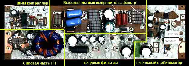
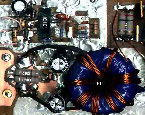
Layout

PCB size is 260*80mm, component footprint 250*60mm. Blue snowflakes mark mounting holes for the three heat-sinked FETs - they are soldered under the board. Total heatsink requirement is under 10W. All HV network is surface-mounted on the upper side (no vias or through-holes). T101,102 drains are soldered to 8*15mm contact pads on the upper side. Hot leads of transformer primary and snubber R's are soldered to this pads too. Note that C105, 106 and matching ceramic caps (1uF, SMD type) are placed between T101,102 drains and transformer primary center tap - to minimize AC current loop. The converter works fine with generic (standard ESR) capacitors. The last capacitor (actually - capacitor bank) is not on this board, but on amplifier PCB.


